




ศูนย์ผลิตภัณฑ์
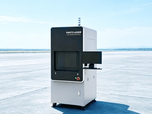
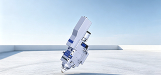
อุปกรณ์เลเซอร์
อุปกรณ์เชื่อมด้วยเลเซอร์
เครื่องเชื่อมด้วยเลเซอร์ระบบหุ่นยนต์
เครื่องเชื่อมด้วยเลเซอร์สำหรับการผลิตยานยนต์
เครื่องเชื่อมด้วยเลเซอร์แบบมือถือ
เครื่องเชื่อมด้วยเลเซอร์ความแม่นยำสูง
เครื่องเชื่อมด้วยเลเซอร์ YAG
เครื่องเชื่อมด้วยไฟเบอร์เลเซอร์
เครื่องเชื่อมพลาสติกด้วยเลเซอร์
เครื่องบัดกรีและเครื่องเชื่อมด้วยเลเซอร์สำหรับงานเฉพาะทาง
ชิ้นส่วนทั่วไป
ติดต่อเรา
อุตสาหกรรมที่ใช้งาน

โซลูชันของ Han's Laser
Han's Laser ให้ความสำคัญกับการวิจัยและพัฒนา (R&D) และนวัตกรรมทางเทคโนโลยีมาโดยตลอด ปัจจุบันเรามีศักยภาพด้านการวิจัยและพัฒนา (R&D) ในอุตสาหกรรมเลเซอร์ระดับชั้นนำของโลก โดยมีสิทธิบัตรมากกว่า 7,400 รายการ ด้วยจุดแข็งด้านผลิตภัณฑ์ เรากำลังขยายโซลูชันครบวงจรที่ครอบคลุมทุกสถานการณ์การใช้งานอย่างต่อเนื่อง เพื่อเสริมศักยภาพให้กับการผลิตอัจฉริยะในหลากหลายอุตสาหกรรมทั่วโลก
ดูทั้งหมด
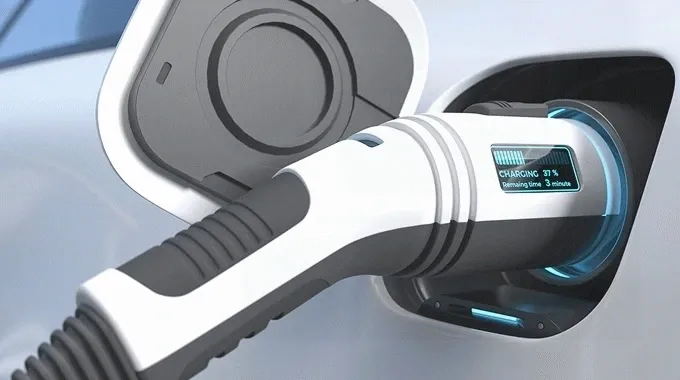
แบตเตอรี่ลิเธียมไอออนสำหรับพลังงานใหม่
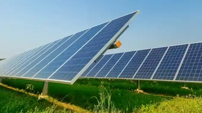
เซลล์แสงอาทิตย์ (PV) และพลังงานแสงอาทิตย์
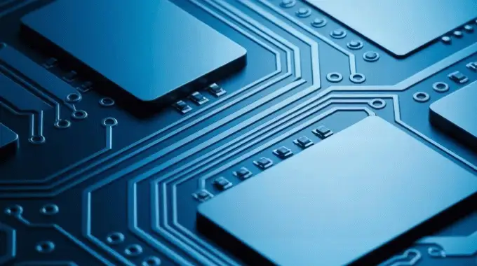
อุตสาหกรรมจอแสดงผลและเซมิคอนดักเตอร์
อุตสาหกรรมแผงวงจรพิมพ์ (PCB)
อุตสาหกรรมอิเล็กทรอนิกส์และสารสนเทศ
อุตสาหกรรมเครื่องจักรกลและโลหภัณฑ์
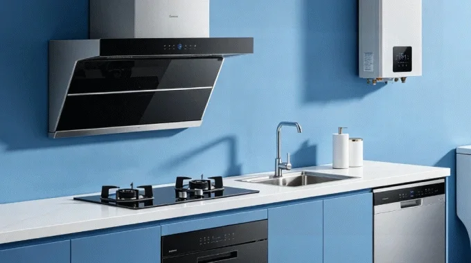
เครื่องใช้ไฟฟ้าภายในบ้านและเครื่องครัว-สุขภัณฑ์
การแปรรูปโลหะแผ่น
อุตสาหกรรมบรรจุภัณฑ์
การคมนาคมขนส่ง
อุตสาหกรรมสิ่งทอและงานตกแต่ง
การผลิตยานยนต์






ติดต่อเรา